Architecture
The new design is a 4-bit architecture rather than an 8-bit architecture like the last version. One thing that complicated my ideas before was trying to figure out how to drive the ALU with a register and another source, latch the ALU output, and write it to the correct place. The new design handles this by using two 74HC670s as 4-bit register sets feeding the ALU directly to avoid the complication of having the ALU on the bus so other sources can drive it. As a result, anything that goes through the ALU needs to be loaded into a register first, which is not a big sacrifice since the two 74HC670s provide eight 4-bit registers. Latching the ALU output also simplifies the design since an instruction only needs to read or write to the ALU but not both in the same instruction. A 74HC574 latch can optionally be trigged to capture the carry bit of the latched ALU output so it can be fed into the next ALU operation.
Other than the ALU and set of four register pairs, there is a 74HC193 counter that supplies the bottom four bits of the address for an 8K SRAM. This register is named X. The next eight bits are supplied by a 74HC574 "RAM pointer." It's a little unconventional to address the memory this way since it splits it into 256 pages of 16 bytes each. However, 16 bytes is the right size for holding floating point numbers, so the memory can be seen as holding 256 objects with the RAM pointer specifying which object. As a bonus, an instruction can trigger the clock input on the X register to count up, saving a few cycles when stepping through memory.
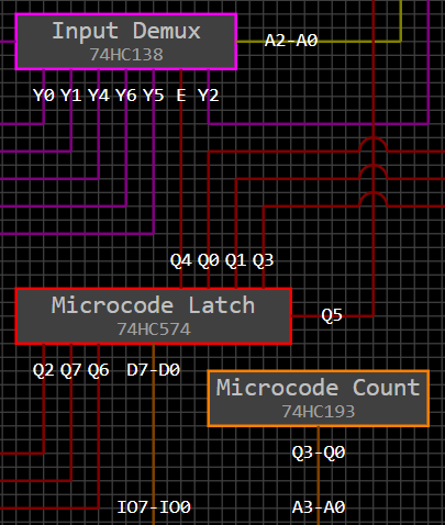
The next part of the system is a 32K EEPROM to hold the program along with four 74HC193 counters to act as the program counter. This is a pretty standard setup. The RAM pointer and X register combo mentioned above drive the EEPROM address through pullups when the program counters are disabled, so constants can be loaded from the program through a 74HC574 latch. Another latch captures instructions from the EEPROM, and a 74HC244 buffer transmits keypad input to the bus. There is also a control signal for an LCD which is connected directly to the output of the two register sets.