Architecture
The new design is a 4-bit architecture rather than an 8-bit architecture like the last version. One thing that complicated my ideas before was trying to figure out how to drive the ALU with a register and another source, latch the ALU output, and write it to the correct place. The new design handles this by using two 74HC670s as 4-bit register sets feeding the ALU directly to avoid the complication of having the ALU on the bus so other sources can drive it. As a result, anything that goes through the ALU needs to be loaded into a register first, which is not a big sacrifice since the two 74HC670s provide eight 4-bit registers. Latching the ALU output also simplifies the design since an instruction only needs to read or write to the ALU but not both in the same instruction. A 74HC574 latch can optionally be trigged to capture the carry bit of the latched ALU output so it can be fed into the next ALU operation.
Other than the ALU and set of four register pairs, there is a 74HC193 counter that supplies the bottom four bits of the address for an 8K SRAM. This register is named X. The next eight bits are supplied by a 74HC574 "RAM pointer." It's a little unconventional to address the memory this way since it splits it into 256 pages of 16 bytes each. However, 16 bytes is the right size for holding floating point numbers, so the memory can be seen as holding 256 objects with the RAM pointer specifying which object. As a bonus, an instruction can trigger the clock input on the X register to count up, saving a few cycles when stepping through memory.
The next part of the system is a 32K EEPROM to hold the program along with four 74HC193 counters to act as the program counter. This is a pretty standard setup. The RAM pointer and X register combo mentioned above drive the EEPROM address through pullups when the program counters are disabled, so constants can be loaded from the program through a 74HC574 latch. Another latch captures instructions from the EEPROM, and a 74HC244 buffer transmits keypad input to the bus. There is also a control signal for an LCD which is connected directly to the output of the two register sets.
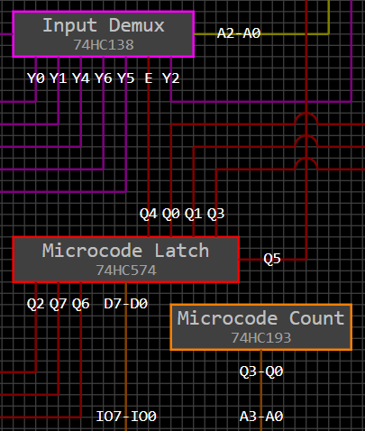
A big problem with the last design was trying to squeeze all of the control signals for the system into just one microcode EEPROM with eight outputs when other designs use two EEPROMs. One idea from the last design to keep the chip count down and fit everything into a calculator was to embed the control signals directly into the program. This made the program balloon in size and caused other problems. The new design keeps all but a few instructions to one byte and still fits everything in just one microcode EEPROM. Here are the signals that the microcode needs to control:
Outputs to Bus Bit 0: ALU latch OE (Output Enable) Bit 1: ROM latch OE Bit 2: RAM OE Bit 3: Keypad input OE Inputs from Bus Bit 4: Carry latch load Bit 5: X register load Bit 6: Program counter load Bit 7: RAM pointer load Bit 8: RAM load Bit 9: LCD load |
Control Signals Bit 10: X register count up Bit 11: Program counter increment Bit 12: Program counter OE Bit 13: ALU latch load Bit 14: ROM latch load Bit 15: Instruction latch load Bit 16: Register sets address bit 0 Bit 17: Register sets address bit 1 Bit 18: Register set 0 load Bit 19: Register set 1 load |
These 20 signals are a lot more than the eight lines the microcode EEPROM can control, so the new design relies on a few tricks to make everything fit. First, the bits of the instruction itself are used to encode some of the signals. Since the instruction byte is just a lookup value into the ALU and microcode EEPROMs, it can encode different information than the microcode. As you can see above, there are four chips that can drive the bus and six that can read from it. Two 74HC138 demultiplexers (one for outputs and one for inputs) driven by the instruction bits allow one source and one destination to be selected for each instruction. Each demultiplexer has three input bits that allow it to activate one of up to eight other chips. In the case of the outputs, only two of the three input bits to the demultiplexer are needed since there are only four chips to select from, yet all three are used. When the second half of the outputs are selected, none of the outputs drive the bus. Instead, pullups from the instruction bits to the bus allow the inputs to load 4-bit immediate values encoded in the instruction. For convenience's sake, Bit 10, which increments the X register, is treated as the 7th bus input. This leaves about 10 signals left to control with the eight microcode ROM outputs. Bits 16 and 17 which control which of the four register pairs in the 74HC670s is selected can share pins with the program counter increment and instruction latch load signals. Both of those signals start out high for every instruction and go low at least once before the instruction ends, so there's no problem leaving the signals high or bringing them low for a few extra cycles to select the right register. Here's how everything is encoded:
| Chip | Instruction | Microcode | |||||||||||||||
| 7 | 6 | 5 | 4 | 3 | 2 | 1 | 0 | 7 | 6 | 5 | 4 | 3 | 2 | 1 | 0 | ||
| ALU | 5 | 4 | 3 | 2 | 1 | 0 | |||||||||||
| Input Demux | 2 | 1 | 0 | ||||||||||||||
| Output Demux | 2 | 1 | 0 | ||||||||||||||
| 4-bit Immediate | 3 | 2 | 1 | 0 | |||||||||||||
| Register Set 1 Load | 0 | ||||||||||||||||
| Register Set 2 Load | 0 | ||||||||||||||||
| Instruction Latch Load | 0 | ||||||||||||||||
| Register Address | 1 | 0 | |||||||||||||||
| Input Demux Enable | 0 | ||||||||||||||||
| ROM Latch Load | 0 | ||||||||||||||||
| ALU Latch Load | 0 | ||||||||||||||||
| Program Counter OE | 0 | ||||||||||||||||
| Program Counter Increment | 0 | ||||||||||||||||
As you can see, the load signals for the ROM latch and ALU latch are driven directly by the microcode rather than the input demultiplexer that selects which device reads from the bus. It makes sense to devote two of the scarce microcode pins to these two since the ALU is used so often and the ROM latch can be used in jump instructions that need to put 8-bit immediates on the bus.
Some of the ideas from the last post about this project didn't make it into the new design. Pull-up resistors, for example, are only used for loading 4-bit immediates from instructions and using the RAM pointer to drive the program ROM address bus occasionally. Even the RAM pointer could work without pull-ups if the microcode signal to enable the program counter OE can be inverted. It's not worth adding an inverter chip for this since the design should be as small as possible, but there might be a spare inverter to use if a 74HC04 chip with six inverters is needed for the clocking system. Another idea is to pull the outputs of the RAM pointer down so that when the chip is disabled, accesses to RAM will be specified by the X register. This would let me use the first 16 addresses of RAM like storage registers while leaving the RAM pointer value intact. There doesn't seem to be an easy way to do this, though, since there are no more microcode pins free. One idea would be to drive the OE of the RAM pointer with one of the bits of the microcode counter so that it's output is available on some cycles and disabled on others.
The last thing left to figure out for the architecture is what to do with some of the unused and undriven pins. A12 of the microcode ROM address bus is not driven, so it will need to be pulled down or attached to something else which would allow for two sets of microcode. One use for this is two processor modes like the decimal mode on the 6502, although that wouldn't be too useful for this project. Another idea is latching the zero flag with the carry flag and feeding both to the ALU. A12 of the data RAM is also not driven, so only 4K of the 8K are accessible with the RAM pointer and X register. Somehow a bit for this will need to be found somewhere so the whole memory can be used. On the other hand, some of the pins that could be useful aren't being used for anything. The input demultiplexer has an extra select signal that could be used for something. The program counter is 16 bits, although only 15 are used for the 32K program ROM. The carry latch only latches one bit from the ALU latch, so there may be some way to use the other seven for the missing signals for the microcode ROM and data RAM address pins.
Schematic
A big part of documenting the project is creating a schematic. It's also helpful to see everything laid out while working on the design. None of the software I've tried for making high-level schematics has done exactly what I wanted, so I decided to make a Python script to do it. The script reads in a text file which describes all the chips and connecting wires and outputs an SVG file of the schematic. The text file is written in a stack-based language like Forth that is very easy to parse, so the Python script only took about a day to write. That's less time than I might have spent learning other software packages without the guarantee that any of them would work, so I consider it time well spent. The SVG file of the schematic is hosted on my local Linux server, so I can see the output in a browser window on my laptop every time the schematic updates.
The text file describing the schematic uses words like CHIP and WIRE that begin a description. Each new object starts out with the same X, Y coordinates as the last one and can be moved absolutely or relative to other objects. This is really helpful when several objects need to be moved and keep their spacing since only the position of one object needs to be modified in the text file and the other objects positioned relative to it move as well. Here's an example:
2 MARGIN ;Margin around schematic
16 4 "74HC193" SIZE ;Define sizes of chips used below
20 4 "74HC244" SIZE
BLUE BORDER-COLOR ;Border color for new chips
CHIP
"Foo" NAME
"74HC244" MODEL
END
CHIP
"Bar" NAME
"74HC193" MODEL
RED BORDER-COLOR
FOO.BOTTOM Y ;Set Y of Bar to bottom edge of Foo
4 DOWN ;Move Bar 4 squares down
LAST.RIGHT X ;Set X to right edge of Foo ("LAST" refers to last chip)
END
0 128 0 RGB WIRE-COLOR ;Wire color dark green
WIRE
FOO.BOTTOM Y ;Wire starts at bottom center of Foo
FOO.X-CENTER X MARK ;Mark beginning of wire
1 DOWN POINT ;Go down 1 square and draw a wire from last point
"Output" LABEL ;Create a label called Output
BAR.Y-CENTER Y ;Wire down to vertical center of Bar
POINT
BAR.LEFT X 2 LEFT ;Wire right almost to Bar
POINT
"Input" LABEL
BAR.LEFT X POINT ;Finish wire to Bar
END

It only took a few days to finish the design. After it was done, new ideas continued to come to me, although I didn't go back to modify the schematic every time. That's why there's an extra chip called "Register Selector" in the schematic below, for example, even though it was eliminated. When I eventually get to build the hardware, I'll update the schematic to reflect the actual design.
Click the thumbnail below for full SVG image

Instructions
Planning out the instruction set for this project was really fun! One thing still uncertain is how to name the registers. Each instruction can refer to one of four pairs of 4-bit registers. Since there are four pairs, they could be called A, B, C, and D, for example. The low part of register A would then be AL and the high part AH, but this is a little too close to the naming of x86 registers. Another idea is to name them R0-R3 with the low part of R0 called R0L and the high part R0H. I'm not sure this is the best way to name them, but it's how they are referred to below. Here are the different types of instructions:
Loading data on the bus (15 instructions, 1 byte)
These instructions move data from one of the four chips that can drive the bus to one of four that can read from it. Moving from RAM to RAM is not allowed.
Outputs to bus ALU latch ROM output RAM Keyboard input |
Inputs from bus X register RAM RAM pointer Carry latch |
Loading registers from the bus (48 instructions, 1 byte)
These instructions load the registers from the four chips that can drive the bus. Because the microcode has separate load signals for the two halves of each register, instructions can load data from the bus into either 4-bit half of the register or both halves at once.
Outputs to bus ALU latch ROM output RAM Keyboard input | Inputs from bus R0, R1, R2, R3 R0L, R1L, R2L, R3L R0H, R1H, R2H, R3H |
Loading 4-bit constants (48 instructions, 1 byte)
These instructions use four bits encoded in the instruction itself to drive the bus. They can load either half of R0 with a single 1-byte instruction, so loading an 8-bit constant only takes two bytes. They can also load the X register which holds four bits.
Outputs to bus #0-#0xF | Inputs from bus R0L, R0H X register |
Loading 8-bit constants (8 instructions, 1 byte)
Both the low and high half of the data bus are pulled up by the same four bits of the instruction, so latching in eight bits at a time sets both halves to the same value. The only useful values of this form are 0 and 0xFF. Moving 0 or 0xFF to the carry latch accomplishes set and clear carry.
Outputs to bus #0, #0xFF | Inputs from bus R0 RAM RAM pointer Carry buffer |
Incrementing the X register (5 instructions, 1 byte)
These instructions increment the X register. The register loading instructions only work with R0-R2 because the instruction for loading R3 would conflict with part of the instruction map used by the ALU. However, if loading R3 turns out to be more useful, the microcode can be changed to support it at the expense of one ALU operation.
Increment X
Increment X by two
Move RAM to R0 and increment X
Move RAM to R1 and increment X
Move RAM to R2 and increment X
ALU operations that work with R0 (16 instructions, 1 byte)
With 64 ALU operations, there isn't enough room in the instruction set for a copy that works with each of the four main registers, so most operations only work with R0. The low and high halves of the register form the two arguments, and the result is written to the ALU latch rather than being immediately written back to the register. Some instructions like divide and multiply might work better assigned to a different register to free up R0 for other tasks.
Add carry only
Add without carry
Bitwise AND
Bitwise OR
Bitwise XOR
Decimal add carry only
Decimal add without carry
Decimal decrement
Decimal divide
Decimal increment
Decimal multiply
Decimal round
Decimal subtract without carry
Rotate left
Rotate right
Subtract without carry
ALU operations that work with R0-R3 (44 instructions, 1 byte)
Although there isn't enough room in the instruction set for every ALU operation to work with all four registers, it makes sense to let the most important ones work with all of them.
Add
Decimal add
Decimal subtract
Decrement nibbles as byte
Decrement nibbles separately
Increment nibbles as byte
Increment nibbles separately
Move value to ALU latch unmodified
Move value to ALU latch with high and low nibbles swapped
Move value to ALU latch with high and low nibbles swapped and write back to register
Subtract
ALU constant lookups (6 instructions, 1 byte)
Since the ALU is a lookup table in an EEPROM, some of the instructions can yield constants based on an index rather than performing calculations. This will save firmware space and work faster than loading the constants out of ROM with a pointer. It should work really well for CORDIC calculations and jump tables for stack operations.
Convert character to index for character drawing
Load character data based on index
Load CORDIC constant
Load jump table address - low byte
Load jump table address - high byte
Load misc constant (pi, e, etc)
Jumps (3 instructions, 1-2 bytes)
Jumps were one of the things I didn't find a good solution for in my last design. This one makes it easy to perform jumps from several sources. As it is now, at least one byte of the address will need to transit a register. If needed, the value in the register before the jump can be stored in the ALU latch and written back to the register after the jump.
Jump to address stored in RAM
Jump to address stored in ROM
Jump to address stored in registers
Conditional jumps (5 instructions, 1 byte)
Like absolute jumps, conditional jumps were something that didn't make it into the old design. My thought was to use an AND or OR gate with one of the processor flags and the load pin on the program counters, which would have required an extra chip. The new idea is to set the carry flag depending on the result of a comparison operation. A second instruction adds two to the current address held in a register depending on the state of the carry then jumps to the address. Execution will continue on the next line or skip two bytes which is enough room for a jump instruction. The original carry can be saved to a register in case it needs to be retained after the jump.
Set carry if result was zero
Set carry if result was greater than zero
Set carry if result was greater than or equal to zero
Add two to address if carry set
Add two to address if carry not set
Writing to the LCD (3 instructions, 1 byte)
Write data in R0 to LCD
Write data in R1 to LCD
Write data in R0 to LCD twice
Miscellaneous (2 instructions, 1 byte)
No operation
Latch ROM output
Undefined instructions (52 instructions)
52 undefined instructions leaves a lot of room for expansion. There is room for 13 more ALU operations, and several of those could work with all four registers. As the calculator firmware develops, I'll be able to add instructions and make modifications.
Instruction Matrix
ALU operations are in cyan and shadowed ALU operations are in green.
| Op code | Instruction | Op code | Instruction | Op code | Instruction | Op code | Instruction | |
| 0x0 | 0x40 | CONST CORDIC | 0x80 | 0xC0 | ||||
| 0x1 | 0x41 | CONST TABLE1 | 0x81 | 0xC1 | ||||
| 0x2 | MOV R0,@RP+ | 0x42 | CONST TABLE2 | 0x82 | MOV R1,@RP+ | 0xC2 | MOV R2,@RP+ | |
| 0x3 | 0x43 | CONST OTHER | 0x83 | INX | 0xC3 | INX2 | ||
| 0x4 | MOV R0L,#0 | 0x44 | MOV R0L,#4 | 0x84 | MOV R0L,#8 | 0xC4 | MOV R0L,#12 | |
| 0x5 | MOV R0L,#1 | 0x45 | MOV R0L,#5 | 0x85 | MOV R0L,#9 | 0xC5 | MOV R0L,#13 | |
| 0x6 | MOV R0L,#2 | 0x46 | MOV R0L,#6 | 0x86 | MOV R0L,#10 | 0xC6 | MOV R0L,#14 | |
| 0x7 | MOV R0L,#3 | 0x47 | MOV R0L,#7 | 0x87 | MOV R0L,#11 | 0xC7 | MOV R0L,#15 | |
| 0x8 | MOV X,A | 0x48 | ALU Free | 0x88 | MOV R0L,A | 0xC8 | MOV R2L,A | |
| 0x9 | MOV X,ROM | 0x49 | ALU Free | 0x89 | MOV R0L,ROM | 0xC9 | MOV R2L,ROM | |
| 0xA | MOV X,@RP | 0x4A | ALU Free | 0x8A | MOV R0L,@RP | 0xCA | MOV R2L,@RP | |
| 0xB | MOV X,IN | 0x4B | ALU Free | 0x8B | MOV R0L,IN | 0xCB | MOV R2L,IN | |
| 0xC | MOV X,#0 | 0x4C | MOV X,#4 | 0x8C | MOV X,#8 | 0xCC | MOV X,#12 | |
| 0xD | MOV X,#1 | 0x4D | MOV X,#5 | 0x8D | MOV X,#9 | 0xCD | MOV X,#13 | |
| 0xE | MOV X,#2 | 0x4E | MOV X,#6 | 0x8E | MOV X,#10 | 0xCE | MOV X,#14 | |
| 0xF | MOV X,#3 | 0x4F | MOV X,#7 | 0x8F | MOV X,#11 | 0xCF | MOV X,#15 | |
| 0x10 | JREG | 0x50 | JC2 R3 | 0x90 | MOV R0H,A | 0xD0 | MOV R2H,A | |
| 0x11 | JROM | 0x51 | AND R0 | 0x91 | MOV R0H,ROM | 0xD1 | MOV R2H,ROM | |
| 0x12 | JRAM | 0x52 | OR R0 | 0x92 | MOV R0H,@RP | 0xD2 | MOV R2H,@RP | |
| 0x13 | Latch ROM | 0x53 | XOR R0 | 0x93 | MOV R0H,IN | 0xD3 | MOV R2H,IN | |
| 0x14 | MOV R0H,#0 | 0x54 | MOV R0H,#4 | 0x94 | MOV R0H,#8 | 0xD4 | MOV R0H,#12 | |
| 0x15 | MOV R0H,#1 | 0x55 | MOV R0H,#5 | 0x95 | MOV R0H,#9 | 0xD5 | MOV R0H,#13 | |
| 0x16 | MOV R0H,#2 | 0x56 | MOV R0H,#6 | 0x96 | MOV R0H,#10 | 0xD6 | MOV R0H,#14 | |
| 0x17 | MOV R0H,#3 | 0x57 | MOV R0H,#7 | 0x97 | MOV R0H,#11 | 0xD7 | MOV R0H,#15 | |
| 0x18 | MOV RP,A | 0x58 | JC1 | 0x98 | MOV R0,A | 0xD8 | MOV R2,A | |
| 0x19 | MOV RP,ROM | 0x59 | CA | 0x99 | MOV R0,ROM | 0xD9 | MOV R2,ROM | |
| 0x1A | MOV RP,@RP | 0x5A | ASCII | 0x9A | MOV R0,@RP | 0xDA | MOV R2,@RP | |
| 0x1B | MOV RP,IN | 0x5B | ALU Free | 0x9B | MOV R0,IN | 0xDB | MOV R2,IN | |
| 0x1C | MOV RP,#0 | 0x5C | DOC | 0x9C | 0xDC | |||
| 0x1D | MOV A,R0 | 0x5D | MOV A,R1 | 0x9D | MOV A,R2 | 0xDD | MOV A,R3 | |
| 0x1E | MVS A,R0 | 0x5E | MVS A,R1 | 0x9E | MVS A,R2 | 0xDE | MVS A, R3 | |
| 0x1F | 0x5F | DMUL R0 | 0x9F | 0xDF | MOV RP,#$FF | |||
| 0x20 | MOV @RP,A | 0x60 | DDIV R0 | 0xA0 | MOV R1L,A | 0xE0 | MOV R3L,A | |
| 0x21 | MOV @RP,ROM | 0x61 | STICKY R0 | 0xA1 | MOV R1L,ROM | 0xE1 | MOV R3L,ROM | |
| 0x22 | NOP | 0x62 | ROUND R0 | 0xA2 | MOV R1L,@RP | 0xE2 | MOV R3L,@RP | |
| 0x23 | MOV @RP,IN | 0x63 | ROR R0 | 0xA3 | MOV R1L,IN | 0xE3 | MOV R3L,IN | |
| 0x24 | MOV @RP,#0 | 0x64 | ROL R0 | 0xA4 | 0xE4 | |||
| 0x25 | INC4 R0 | 0x65 | INC4 R1 | 0xA5 | INC4 R2 | 0xE5 | INC4 R3 | |
| 0x26 | INC8 R0 | 0x66 | INC8 R1 | 0xA6 | INC8 R2 | 0xE6 | INC8 R3 | |
| 0x27 | 0x67 | AOC | 0xA7 | 0xE7 | MOV @RP,#$FF | |||
| 0x28 | SWAP R0 | 0x68 | SWAP R1 | 0xA8 | SWAP R2 | 0xE8 | SWAP R3 | |
| 0x29 | DEC44 R0 | 0x69 | DEC44 R1 | 0xA9 | DEC44 R2 | 0xE9 | DEC44 R3 | |
| 0x2A | DEC8 R0 | 0x6A | DEC8 R1 | 0xAA | DEC8 R2 | 0xEA | DEC8 R3 | |
| 0x2B | 0x6B | ALU Free | 0xAB | 0xEB | ||||
| 0x2C | MOV R0,#0 | 0x6C | DDEC8 R0 | 0xAC | LCD R0 | 0xEC | LCD R1 | |
| 0x2D | 0x6D | ALU Free | 0xAD | 0xED | ||||
| 0x2E | 0x6E | ALU Free | 0xAE | 0xEE | ||||
| 0x2F | 0x6F | DINC8 R0 | 0xAF | LCDx2 R0 | 0xEF | MOV R0, #$FF | ||
| 0x30 | MOV C,A | 0x70 | ADD R0 | 0xB0 | MOV R1H,A | 0xF0 | MOV R3H,A | |
| 0x31 | MOV C,ROM | 0x71 | SUB R0 | 0xB1 | MOV R1H,ROM | 0xF1 | MOV R3H,ROM | |
| 0x32 | MOV C,@RP | 0x72 | DADD R0 | 0xB2 | MOV R1H,@RP | 0xF2 | MOV R3H,@RP | |
| 0x33 | MOV C,IN | 0x73 | DSUB R0 | 0xB3 | MOV R1H,IN | 0xF3 | MOV R3H,IN | |
| 0x34 | CLC | 0x74 | GT | 0xB4 | 0xF4 | |||
| 0x35 | 0x75 | GTE | 0xB5 | 0xF5 | ||||
| 0x36 | 0x76 | EQ | 0xB6 | 0xF6 | ||||
| 0x37 | 0x77 | ALU Free | 0xB7 | 0xF7 | SEC | |||
| 0x38 | 0x78 | ALU Free | 0xB8 | MOV R1,A | 0xF8 | MOV R3,A | ||
| 0x39 | 0x79 | ALU Free | 0xB9 | MOV R1,ROM | 0xF9 | MOV R3,ROM | ||
| 0x3A | 0x7A | ALU Free | 0xBA | MOV R1,@RP | 0xFA | MOV R3,@RP | ||
| 0x3B | 0x7B | ALU Free | 0xBB | MOV R1,IN | 0xFB | MOV R3,IN | ||
| 0x3C | ADC R0 | 0x7C | ADC R1 | 0xBC | ADC R2 | 0xFC | ADC R3 | |
| 0x3D | SBC R0 | 0x7D | SBC R1 | 0xBD | SBC R2 | 0xFD | SBC R3 | |
| 0x3E | DADC R0 | 0x7E | DADC R1 | 0xBE | DADC R2 | 0xFE | DADC R3 | |
| 0x3F | DSBC R0 | 0x7F | DSBC R1 | 0xBF | DSBC R2 | 0xFF | DSBC R3 |
Assembler
My plan for the assembler is to have every line of source start with an instruction or keyword then have all the arguments use a stack-based format. Also, the source will come before the destination as in MSP430 and AT&T-style x86 assembly for reasons explained below. (I know the Instruction Matrix above has them in the reverse order. I'll update this after the design is finalized.) For example, to load the constant foo plus 2 into R0L, the syntax would look like this:
MOV foo 2 + , R0L ;Write immediate foo+2 to register R0L
As explained above, all of the ALU operations except SWAP write the result to the ALU latch but not to the source register. Storing the result somewhere else like a register or in memory requires a second instruction. For example, adding the two nibbles in R0 and writing the result to R1 would be two separate instructions:
ADD R0 , A ;Add the two nibbles in R0 and write result to ALU latch
MOV A , R1 ;Write result in ALU latch to R1
Since writing anything to the ALU latch is always followed by an instruction writing the result somewhere else, it makes sense to list the two steps on one line even though they are technically two separate instructions:
ADD R0 , R1 ;Add the two nibbles in R0 and write result to R1
Writing the result in the ALU latch somewhere doesn't disturb the value, so it's possible to list multiple destinations in the same instruction:
ADD R0 , @RP X ;Add the nibbles in R0 and write result to RAM and X register
Supporting one source with multiple destinations is why it makes sense to put the source first instead of the destination first like most other forms of assembly such as Intel x86.
Listing multiple destinations is useful for multi-nibble addition since retaining the carry for the next addition is a separate instruction:
ADD R0 , R0 C ;Add the nibbles in R0, write result back to R0, keep carry
I'm not sure yet the best way to distinguish immediates from addresses. Adding a # symbol to immediates like in 6502 assembly or brackets around addresses like in x86 are possibilities though slightly more complex to parse. What appeals to me most now is letting the instruction dictate whether a given number is an immediate or address like in MIPS assembly. In any case, if a number listed as a destination is an address, it would be possible to have an instruction like this:
ADD R0 , FOO BAR 4 + BAZ CAT * 8 +
This instruction has three destinations, although it's hard to tell them apart at a glance. Optional parentheses around each term would clarify things and could check that exactly one item is on the stack per destination to avoid stack underflow or overflow:
ADD R0 , FOO ( BAR 4 + ) ( BAZ CAT * 8 + )
Although I want to stick to syntax that is easy to parse, I think allowing commas and parentheses to be separators like space will be a good compromise:
ADD R0, FOO (BAR 4 +) (BAZ CAT * 8 +)
Conclusion
It was a lot of fun to finally figure out a TTL calculator design that solves all the problems I've been thinking about for the past few years. Now that I have all my ideas recorded for this project, I can go back to the projects I set as goals for myself in 2022. This project will be waiting for when I have time to come back and implement it.
No comments:
Post a Comment