After two and a half years of on and off work, I'm ready to end this project. Unfortunately, I got distracted by other things and never got close to finishing the project. When I last worked on it, the calculator could step through program memory, load immediate values, and move values between registers. The ALU in the form of a DIP8 SPI EEPROM was programmed but never hooked up to the rest of the circuit. A few months ago when I moved, I finally took apart all the breadboards, so the calculator is officially gone. Below are some ideas about what I would like to keep and what I would like to do differently next time if I ever return to this project. Over the past few years, I've thought a lot about how to redesign this, so I may change my mind again. These are the ideas I have so far.
What to keep
Control signals in instructions
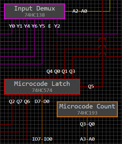
Like most other TTL computers, this one used an EEPROM to store the microcode controlling the state of the components in the system. Since the instruction byte is just an arbitrarily assigned index into a lookup table, I also encoded information in the instruction itself. This let me save room in the design and is part of how everything fit into one microcode EEPROM instead of two.
Work on both sides of the clock
An inverted copy of the clock signal latches values where necessary so that state changes in the circuit when the clock signal goes up and is latched when it goes down. This is simpler than trying to coordinate machine cycles like a Z80 or 8051.
Separate RAM and program memory
As tempting as it is to build a Von Neumann architecture where addresses can refer to RAM or ROM, it's simpler to keep the two types of memory apart.
What to change
Move from 8-bit to 4-bit architecture
This is the biggest change since it affects a lot of the other aspects of the design. It will hopefully require fewer chips and simplify some things. In the old design, for example, there were four 74HC670s that form two sets of four registers for a total of eight 8-bit registers. In the new design, one 8-bit latch should be enough to hold two 4-bit registers. This is also a good register size since the BCD numbers a calculator uses are divided into 4 bits for each decimal place.
Simplify design
The old design was up to over 30 chips without being finished. Space on the two protoboards I planned to put the chips on was starting to get really tight. The new design should be simpler since it only uses 4-bit registers and also because I have some new ideas for reducing the chip count like using pull ups to eliminate a lot of buffers. For example, to load immediate values into one half of the 8-bit latch that holds the two 4-bit registers, the immediate value can be encoded in the instruction and fed to the data bus with pull ups. Z-stating everything that can drive the data bus and loading the latch will load the immediate. The other 4-bit half can drive the other four bits of the data bus so the load retains the value in the other half of the latch. Another idea is to use pullups to the RAM address bus driven by the bits of the instruction to refer to eight or 16 bytes of RAM that can be used like registers.
Arithmetic Logic Unit (ALU)
My plan to use a DIP8 EEPROM as an ALU was something novel about the old design but at the same time also what held me back from finishing it. The EEPROM I found had 4MB of storage, so it could hold 64 tables 8x8 in size. Adding a carry bit, this would mean 32 ALU operations which is definitely enough to implement what I was planning with the calculator. Carry could also serve to refer to different instructions in cases where it isn't used, such as multiply and divide, so the practical number of instructions would be much more than 32. The problem with this setup is getting the 22 bits of information needed for every ALU operation into the EEPROM efficiently along with the eight bits or more needed to put the device into read mode. One idea was to run a second clock eight or 16 times faster than the main clock and use that to clock data into the EEPROM, but I could never figure out how to get the two systems to cooperate while running at different speeds. Also, this setup would require extra latches and shift registers which would probably negate any space savings from using the EEPROM in DIP8. The new design will use a 32KB EEPROM. With eight bits for the two 4-bit registers and one bit for the carry bit, there will be room for 64 ALU operations.
There are a few aspects of this that I haven't figured out yet. One is how to handle the carry bit. The 8-bit latch holding the two 4-bit registers will drive the ALU and also receive it's output, so in the case of addition, one half will contain the sum and the other half will contain the carry. From there, there needs to be some way to record the carry bit since it will be overwritten when a new value is loaded into the register. The easy way is to add a latch to capture the carry, though I hope I can devise something that doesn't add to the chip count like having that latch do something else useful with the other seven bits.
Another interesting advantage of using an 8-bit latch to hold both registers that feed the ALU is that the latch can load an 8-bit address value from ROM or RAM and increment it with the ALU without having to do it in two 4-bit halves. The problem with this is that the ALU output is only 8-bits so there is no room to record the carry output which would be needed to increment a 16-bit pointer. One solution is to keep the 8-bit value in the latch and test if it's zero to know if it overflowed. Another idea is to have a separate bit fed to the ALU so that operations can have a second 8-bit output when needed as in this case with the carry bit. The advantage of this is that 4-bit operations could also have a carry output without trashing one of the two 4-bit registers to hold the carry.
Microcode changes
The old design embedded microcode directly into the program ROM in order to reduce the number of microcode ROMs from two down to one. This made some instructions balloon to many bytes. In retrospect, I don't think even a simple scientific calculator would have fit into the 8KB EEPROM I was using since the encoding was so inefficient. The next design will use a more traditional setup without microcode steps in the program. I'm still trying to think of ways to get away with only one EEPROM for microcode. One idea is to store two 8-bit values on the EEPROM for each microcode step and add a second latch to output the second byte every instruction cycle.
Program Counter (PC)
The program counter is another area that proved to be more difficult than I imagined. For one, connecting three 4-bit counters is a huge amount of wiring and only allows for an 8KB program ROM. Unfortunately, as I mentioned in a previous post, there are no readily available 8-bit counters that can be loaded with an arbitrary value. One simplification is to use two 4-bit counters and an 8-bit latch to allow a full 64KB address space. This would require the last instruction in every 256 byte page of program space to change the 8-bit latch to the next page. The assembler could insert those instructions in the background without the programmer needing to worry about them.
Voltage
The old design used a mixture of 3.3v and 5v since the EEPROMs all need 5v while the DIP8 EEPROM for the ALU needed 3.3v. The next time around, I plan to keep everything the same voltage if possible. Hopefully, this will eliminate the HCT parts I was using for managing level translations.
Simulation
Building this type of TTL computer in a simulator is one of the most fun parts of these projects. The last time, I used Atanua to simulate part of it. Unfortunately, I found a major bug in one of the counter chips that would be used for the program counter. The author of Atanua responded to my email reporting the bug but was not helpful in fixing it since he no longer maintains Atanua. There are also useful chips like the 74HC670 that aren't simulated in Atanua, so I think I would try making my own TTL simulator next time. This would be quite a lot of work which is part of my hesitation to jump back into this project.
Miscellaneous ideas
There are a few other interesting things that might be useful for this project that I haven't found a place for yet. The 74HC670 that I was using for registers before is an amazing chip that I don't have plans for in the new design. Implementing some type of bank switching for the RAM or ROM using this might help reduce a chip or two, though there would have to be a way to set it without adding extra chips.
Another interesting observation is that a latch holding eight bits of an address plus four more bits encoded in an instruction would let me specify 12 bits which is enough to address 4KB of RAM. Since 16 bytes can hold a BCD floating point number, memory could be split up into 256 chunks 16 bytes in size. This could shrink the SRAM addressing mechanism to just one 8-bit latch. The problem is that encoding the lower four bits in the instructions means there is no flexibility to loop through the 16 bytes programmatically, so a different mechanism would be needed for when that's necessary.